Traditional TLM models require stubs to model structures filled with dielectric layers, such as microstrip, finline, etc. Usually, when cubic cells are used to discretize inhomogeneous dielectrics, all cells are of equal size, but those in the dielectric other than air are loaded with stubs to slow down the network velocity and reduce the wave impedance. Since the wavelength is shorter in the dielectric regions, the discretization per wavelength is coarser. That, in turn, causes increased dispersion and coarseness errors. Hoefer and Sautier [1] have proposed a general 2D-TLM algorithm which removes the stubs in dielectric layers. In this project that concept has been extended to the 3D cuboid condensed node.
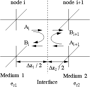
A 3D cuboid condensed node[2] with arbitrary aspect ratios is shown in Fig. 1. This is a unit cell of the generalized three-dimensional TLM network. As discussed in [1] the requirements of impulse synchronism and proper network velocities naturally impose a higher cell density in the dielectric regions. For example, a guiding structure may be uniform in the x-y plane, but consist of two or more dielectric layers in the z direction (see Fig 3.). In this structure, the propagation vectors are the same tangential to the dielectric interface, but different in the normal direction. The discretization in the x-y plane remains the same in both regions, while the discretization in z-direction must be finer in the higher permittivity region. Now we need to determine the aspect ratios of the cells in media 1 and 2. The network velocity is isotropic in both media. One is c / ( 2 sqrt(epsilon_r1) ) and the other is c / ( 2 sqrt(epsilon_r2) ). In addition to satisfying the phase condition at the interface we must also properly represent the impedance step across the interface. The voltage impulses crossing the interface will be scattered as shown in Fig. 2. Based on the above we can simulate inhomogeneous structures without the need for stubs. Since the mesh size in z direction is reduced in the higher permittivity region, dispersion error is reduced accordingly.
To verify the validity and accuracy of the algorithm for the cuboid cell, a parallel plate resonator has been chosen. A TLM implementation has been used to find the resonant frequency. The parallel plate resonator modeled on the computer is shown in Fig. 3. In order to compare the new with the traditional scheme, the resonator has been discretized into cuboid cells of aspect ratios alpha_1 = beta_1 = gamma_1 = 1 in the air layer, yielding alpha_2 = 1, beta_2 = 4 as well as gamma_2 = 1/4 in the dielectric layer (Fig. 4), and into cubic cells with stubs in the dielectric layer. The resonator was excited with a narrow Gaussian impulse, and its response was picked up at two observation points, one in the air region and the other in the dielectric region. Both output points give the same frequency response after Fourier Transform. The numerical results obtained from this simulation are summarized in the following table:
| Theoretical resonant frequency | TLM | |||
|---|---|---|---|---|
| Cuboid node without stubs | Cubic node with stubs | |||
| fr (GHz) | fr (GHz) | error (%) | fr (GHz) | error(%) |
| 5.8355 | 5.8345 | -0.017 | 5.8306 | -0.084 |
| 13.5735 | 13.5622 | -0.083 | 13.5911 | +0.130 |
| 20.0084 | 20.0234 | +0.075 | 20.7177 | +3.545 |
| 25.3538 | 25.2308 | -0.485 | 25.4839 | +0.513 |
| 32.9191 | 32.7659 | -0.465 | 31.6613 | -3.821 |
We thus observe that the cuboid discretization gives better results than the cubic discretization. Based on this comparison, we demonstrate that the cuboid scheme maximizes the flexibility of the TLM method, agrees well with theoretical results, and has better accuracy than the traditional stub-loaded scheme.
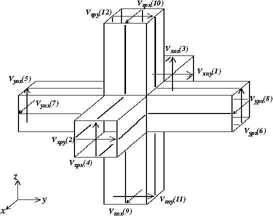
Fig. 1 - 3D cuboid condensed node
Fig. 2 - Impulse scattering at the interface between two dielectric media
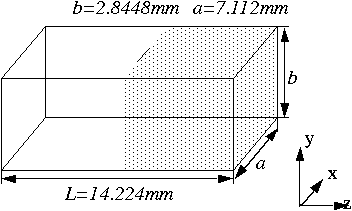
Fig. 3 - Parallel plate resonator
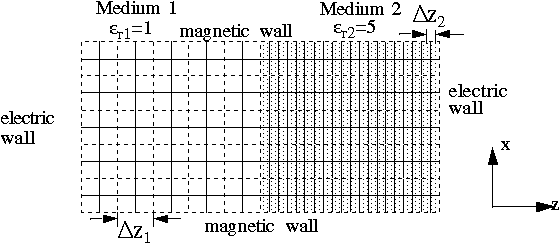
Fig. 4 - Discretization of parallel plate resonator (x-z plane)